Chemical compositions and microstructure of coatings and the coating substrate interfaces
Chemical composition is an essential characteristic of a coating and, in some cases, represents innovative design in order to achieve high performance. For example, multicomponent nitride coatings containing Cr, Al and or Y have significantly enhanced thermal stability and oxidation resistance. By varying the deposition conditions, a transition metal nitride coating can be nitrogen-stoichiometric (e.g. the atomic ratio Ti:N = 50:50 for binary TiN) or sub-stoichiometric or even in the form of Ti2N. In diamond-like carbon (DLC) coatings, doping some metallic elements may lead to remarkable change in the tribological properties.
The microstructure of a coating is usually dramatically different from the bulk material of the same chemical composition, which is attributed to the special growth kinetics. In most cases, vapour deposited coatings exhibit uni-directional microstructure with the elongated grains perpendicular to the coating surface. By varying the growth conditions, e.g. either the energy input or the chemical compositions, the microstructure can be substantially porous, sub-dense or absolutely dense, which is often formed along with specific surface morphology (roughness) and different residual stress condition.
Other specially treated surfaces also have very characteristic microstructure. For example, shot-peening treatments change the surface morphology and generate a depth of plastically deformed structure; carbonizing and nitriding treatments generate compound layers of carbides and nitrides respectively, followed by depths of penetration/diffusion of carbon and nitrogen.
Microstructure is also an important issue for multilayer and composite coatings. In PVD hard coatings, multilayer coatings are grown using multi-cathode sputtering and or arc-evaporation coaters in which the resultant periodic sub-layers possessing different chemical compositions. More recently, nanocomposite coatings comprise nano-scale crystalline grains being embedded in a resin-like medium. Such multilayers and nanocomposite have been found to have outstanding mechanical and tribological properties.
We have the following instrumental techniques to characterize the chemical compositions, microstructure and interfaces of coatings.
SEM is the mostly used microscopic analysis of microstructure. For coatings and surfaces, the field-emission-gun SEM provides a large range of magnifications, typically from 100x to 200,000x, which provides the feasibility to observe the microstructure and surface features from micrometer to manometer scales in one instrument. The mostly common SEM observations of coatings and surfaces include both surface morphology and cross-sectional microstructure, often with complementary EDX analysis as described before.
TEM is the best tool to analyse nano/atomic scale structural characteristics of coatings and surfaces. In MERI, we have the expertise and instrumental conditions in cross-sectional TEM based characterization of various coatings, such as tool coatings, thermal barrier coatings for turbines, as well as nitrided steels. A necessary skill for TEM analysis is the preparation of cross-sectional and plane-view TEM samples. The preparation methods are available in MERI, seeing the relevant webpage
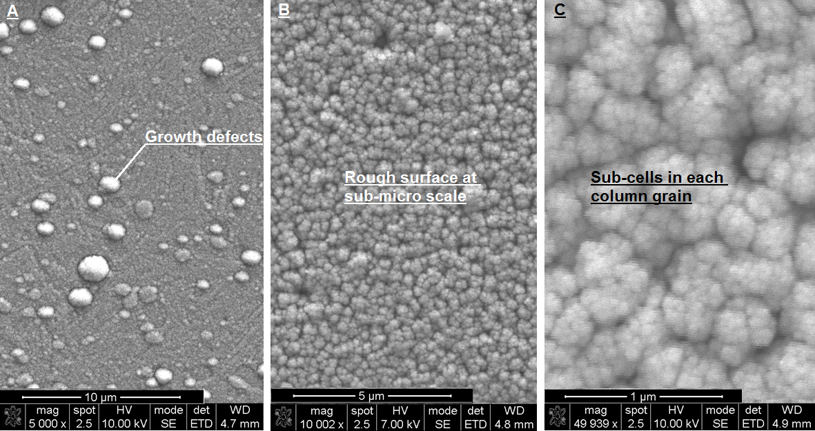
Figure 1 SEM observations of a magnetron sputtered nitride coating TiAlN/VN at three different magnifications: (a) Low magnification observations show generally the flat coating surface having a dispersion of growth defects. (b) When observing at the higher magnification, the coating surface can be evaluated for its smoothness in which the resultant roughness features are known to be related to the growth mode. (c) When the instrument was operated at extremely high magnifications reaching its limit of spatial resolution, it is available to resolve the nano-scale sub-cells on the top of every columnar grain. More details of the sub-grains can be further characterized using TEM.
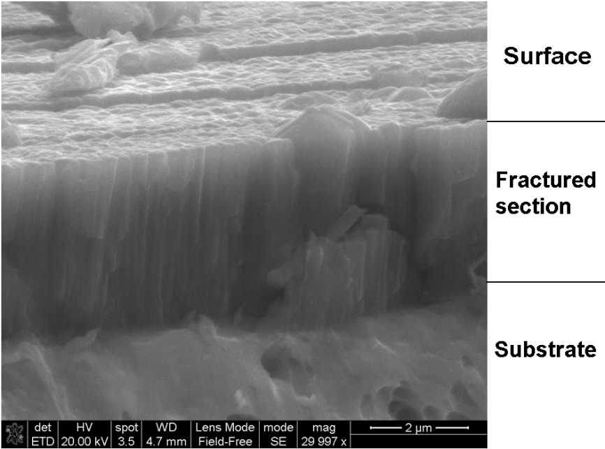
Figure 2 A 3-D view of a fractured section of a sputtered nitride coating grown on a tool steel substrate. The coating is about 3 mm thick, having dense columnar growth structure and sub-micro scale rough surface. A growth defect is shown in front of the fractured edge. Such defects have been found to be initiated by metal-drops emitted from the cathodes during the ion-etching stage prior to the coating deposition.
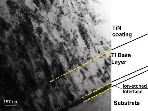
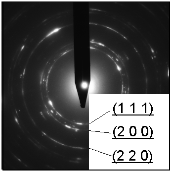
Figure 3 A cross-sectional TEM bright field (BF) image and a pattern of selected area diffraction (SAD) of a magnetron (HIPIMS/DC) sputtered TiN coating. The BF micrograph shows the layered microstructure development from the substrate, ion-etched interface, a Ti-metal base-layer and the TiN topcoat. The coating exhibits dense columnar microstructure without any inter-column voids. The SAD pattern suggests single-phase cubic crystalline structure of the TiN.
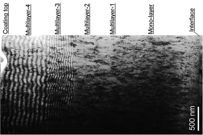
Figure 4 A Cross-sectional TEM BF image of a DC magnetron sputtered nitride coating. The coating was grown in a well-designed program to fabricate various multilayer structures having bi-layers of TiN and MoN. Cross-sectional TEM provides the best spatial resolution in observing such multilayer architectures.
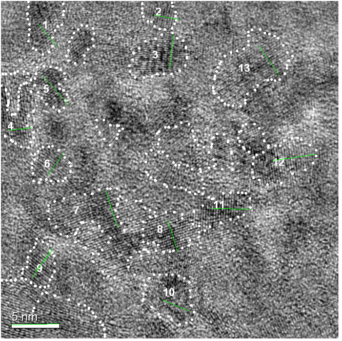
Figure 5 A high-resolution TEM micrograph of a nanocomposite TiSiCN coating grown by plasma enhanced magnetron sputtering. The image was taken at an extremely high magnification and at phase-contrast mode to show short-range ordered domains (nano-crystals), that nanoscale TiN-type grains are embedded in the resin-like Si-C-N medium
The energy dispersive X-ray spectroscopy (known as EDX or EDS) is an attached analytical tool to the three SEM and the TEM. The SEM-EDX analysis is straight forward to reveal the chemical compositions of a coating simultaneously in observing the microstructure or morphology of a coating. The analysis can be either qualitative to tell the presence of most elements (> boron, No. 5 in the Element Periodic Table), and or quantitative to tell the atomic and weight percentages of the detected elements. In addition, the SEM-EDX analysis is also available to make line scans and 2-dimentional mapping analyses to reveal the profiles of specific elements in the microstructure.
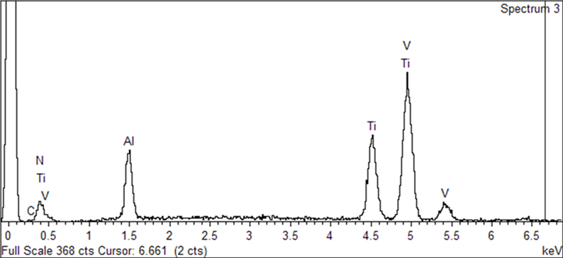
Figure 6 An EDX spectrum of magnetron sputtered TiAlN/VN coating. Note the overlapping of the N-K and Ti-L lines at the energy range 0.4 – 0.5 KeV.
Moreover, one should note the limitations of SEM-EDX analyses. Firstly, the analysis of light elements, including B, C, N and O, is only qualitative with much weaker signals because of the strong absorption of the low-energy characteristic X-rays in the medium. Secondly, EDX spectra should be interpreted by considering the overlapping of some characteristic X-ray signals, such as the overlapping between N and Ti, O and Cr or V, and Mo and S. We have the expertise to support the correct interpretation of the data. Thirdly, the spatial resolution of SEM-EDX analysis is in a scale of a few microns, which is typically not as good as the mostly used secondary electron image. The reduced resolution is due to the fact the excited characteristic X-rays are generated not only within the surface area directly receiving the focused electron beam, but also from a pear-shape volume of substantially larger diameter beneath the surface.
These limitations can be overcome by using TEM based EDX analyses. TEM-EDX analysis is available in MERI, which is able to make point spectroscopic analysis on specially prepared (extremely thin, 0.05 – 0.10 mm in thickness)samples. TEM-EDX analysis is much superior to SEM-EDX in analysing light elements and in analysing the chemical compositions of extremely small objects. For example, TEM-EDX analyses have been applied to characterize the ion-etching induced element-concentration at the interface between a coating and its substrate, the oxidation scales formed on transition metal nitride coatings, as well as tribo-oxidation wear mechanisms.
Additionally, X-ray diffraction (XRD) is applied to characterize the crystalline properties of coatings. In addition to the essential function of XRD in clarifying the crystalline phase compositions, it is able to determine the texture (preferred growth orientation) and residual stresses. For PVD hard nitride coatings, for example, the texture and residual stress properties have significant influence on the tribological and mechanical properties. A few examples of the analyses can be found in the references below.
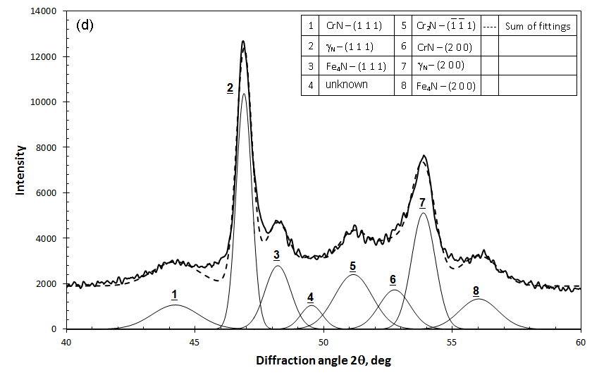
Figure 7 A XRD curve of plasma nitrided 316 austenitic stainless steel. The crystalline phases of the nitrided surface layer is predominantly nitrogen-supersaturated austenite, also known as ‘S-Phase’ or expanded austenite. Using a Gaussian multiple peak-fitting technique, we have undertaken further interpretation of the diffraction pattern. The nitrided layer was found to contain nano-scale clutters of CrN, Cr2N and Fe4N embedded in the austenite parent phase.
MERI also has the secondary ion mass spectroscopy (SIMS) facility to analyse the chemical compositions of a solid surface. By applying ion sputtering on the surface to be analysed, the emitted secondary ions are detected to tell the chemical compositions. SIMS is also capable of analysing the depth profiles of elements.
For more information, please email us at meri@shu.ac.uk or call the MERI Reception on 0114 225 3500.