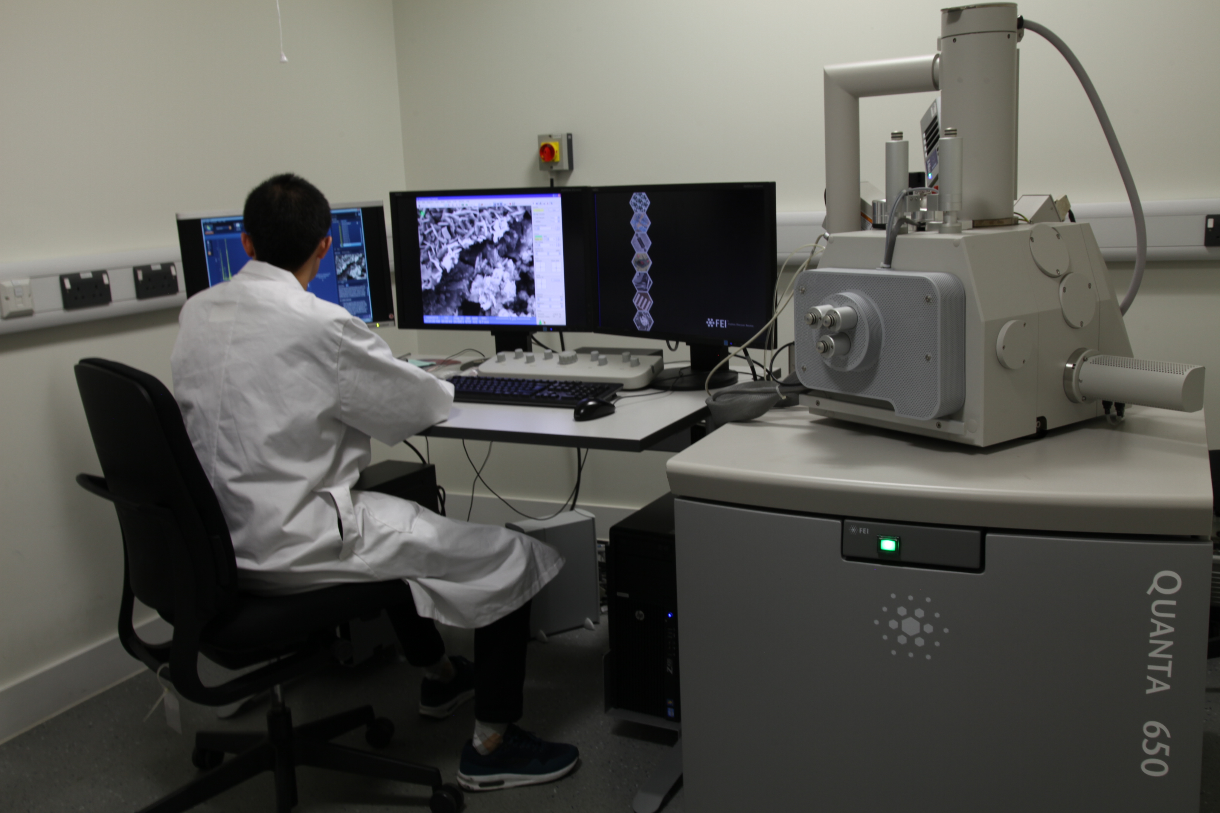
Scanning Electron Microscopy (SEM)
SEM is one of the most useful tools available to materials scientists.
In SEM operation, the sample is put in the vacuum chamber of the microscope and a fine beam of high energy electrons is scanned across a small area. During the scan, interactions between the incident electron beam and the sample surface lead to several types of emissions, including secondary electrons, back-scattered electrons, and characteristic X-rays.
Emissions are detected by different detectors to produce several imaging modes
- the secondary electron image for the surface morphology of the scanned area
- the back-scattered electron image for compositional mass profile
- the characteristic X-rays for energy dispersive spectroscopic chemical analysis.
SEM is a very versatile analytical instrument having up to nm-scale spatial resolution. Analytical SEM is extensively used in various types of materials characterisation and failure investigations.
Why SEM is so useful
- It can give wide range of magnifications from 100× to 100,000× or even higher depending on sample material and the instrumental spatial resolution
- SEM has great depth-of-focus which allows imaging of rough surfaces such as fractures, as-machined surfaces, corrosion and wear of materials, micro-/nano-scale particles, etc
- With little or no need of sample preparation, a wide range of materials can be analysed on SEM, eg conductive/semi-conductive/insulating materials, particles/fibres/blades, various types of coatings, thin films and surfaces
Instruments

MERI currently has four SEM instruments
- FEI NOVA 200 NanoSEM
- Philips XL-40 SEM
- CamScan SEM
- FEI Quanta 3D FEG/FIB ESEM
Please visit the SEM instruments page to view main features and services.
Cases of applications
The SEM instruments are available for wide range of research and industrial consultancy services. Selected cases are listed below
- Laser clad carbide/metal composite coating
- Examination of metallurgical defects
- Characterisation of insulating fibres and powders
- Characterisation of thermal barrier coatings (TBC)
- Characterisation of PVD hard coatings
- Wear failures of machining tools
- Fractography: Corrosion fatigue failure of a stainless steel stud
- Fractography: Fracture failure of a med-carbon steel screw thread
To find out more services we can provide please submit your enquiry or contact us on 0114 225 3500
